The construction of a focused ion beam fib workstation is similar to that of an electron microscope.
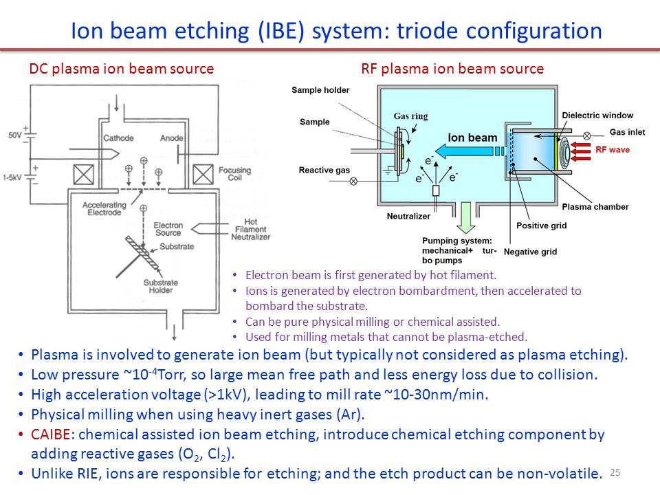
Ion beam etching working principle.
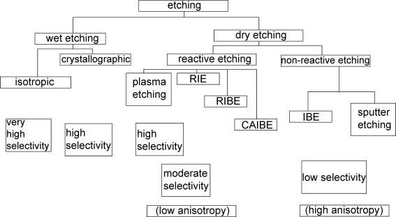
Rie is a type of dry etching which has different characteristics than wet etching.
Ion beam etching also known as ion beam milling or ion milling is the most widely used etching method for preparing solid state samples for scanning electron microscopy sem applications.
It is consists of an electron gun that discharging free electrons into a chamber filled with argon gas.
The probe is fixed on a multi axis tilt stage located in a high vacuum chamber.
The gas is then ionized by the electrons.
Ion beam etching or milling is achieved by directing a beam of charged particles ions at a substrate with a suitably patterned mask in a high vacuum chamber.
High energy ions from the plasma attack the wafer surface and react with it.
It enables highly directional beams of neutral ions to control over the sidewall profile as well as radial uniformity optimisation and feature shaping during nanopatterning.
Each bombarding ions as a result of the collision dislodges the surface layer.
This process is very simple.
It is also called the etching process.
The top of the chamber is called an ion beam generating apparatus.
Not dissimilarly to what happens with sputtering targets the sample material is removed by energy transfer between the accelerated ar atoms and the sample surface.
Ion beam machining diagram it consists of an electron gun which discharges free electrons into a chamber filled with argon gas.
In this process the sample material is bombarded with high energy argon ion beams in a high vacuum chamber.
Rie uses chemically reactive plasma to remove material deposited on wafers.
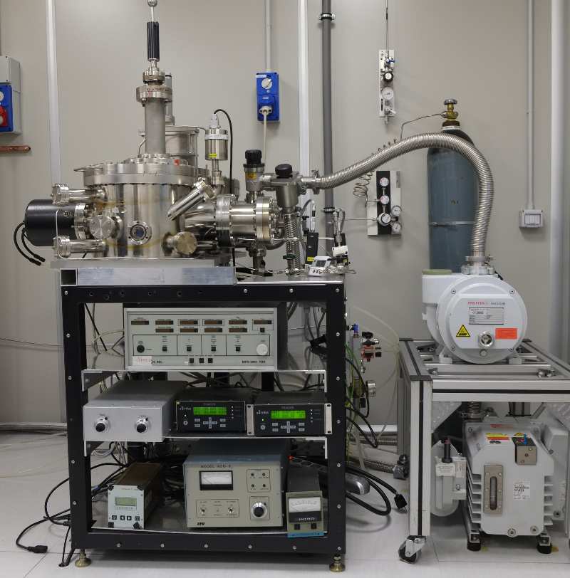
Dual beam machine 22 05 2015 en seminar 5 fib nano machining machining sputtering milling chemically assisted deposition and etching gas injection system ion beam induced imaging se and si micromanipulation of small objects 2 µm 2 µm 200 nm 2 µm.
Inside the column ions are generated accelerated and focused.
However while the sem uses a focused beam of electrons to image the sample in.
Reactive ion etching is an etching technology used in microfabrication.
Focused ion beam also known as fib is a technique used particularly in the semiconductor industry materials science and increasingly in the biological field for site specific analysis deposition and ablation of materials a fib setup is a scientific instrument that resembles a scanning electron microscope sem.
This is a different process from electric discharge electron beam laser beam and plasma arc machining.
The principle of ion beam machining is it consists of bombarding the work with accelerated ion which collides with the surface atoms of the work.
The ion column is connected to this chamber.

.jpg)